- 您现在的位置:买卖IC网 > Sheet目录346 > NCP5680MUTXG (ON Semiconductor)IC LED DRIVER WHT HI EFF 24-UQFN
�� �
�
�NCP5680�
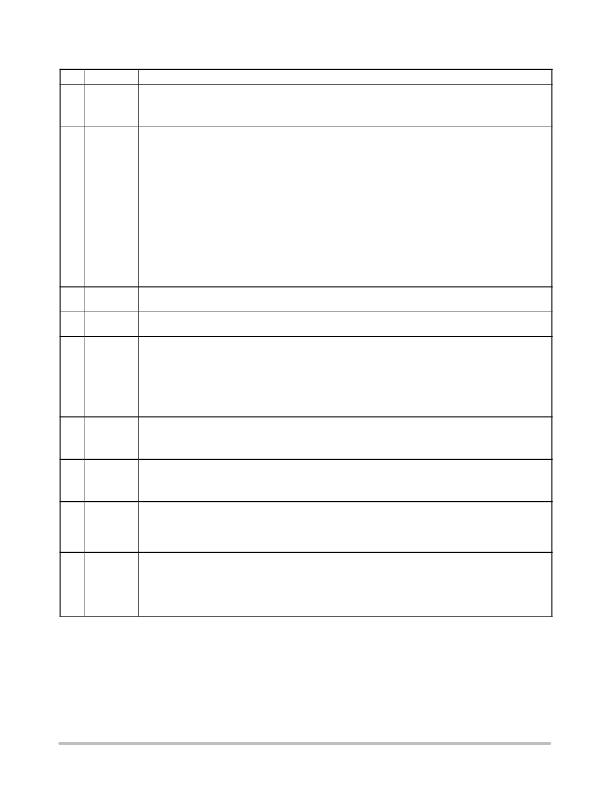
�PIN� DESCRIPTIONS�
�Pin�
�1�
�2�
�Name�
�VSD�
�PHSEN�
�Type�
�OUTPUT,�
�POWER�
�INPUT,�
�ANALOG�
�Description�
�This� pin� provides� the� 2.5� V� Photo� sense� bias� voltage.� The� bias� voltage� is� connected� when� either�
�a� flash� sequence� has� been� selected,� or� the� ENPH� bit,� in� the� CONFIG0� register,� is� set� High.� The�
�output� current� is� limited� to� 1� mA.� The� same� pin� is� used� to� synchronize� the� charge� pump� operation�
�by� an� external� digital� signal� (see� Figure� 6).�
�This� pin� fulfills� two� functions:�
�PHOTO� SENSE� FUNCTION:� the� pin� is� connected� to� the� external� photo� transistor.� The� operating�
�voltage� is� limited� in� the� 0� V� to� 1.7� V� range.� The� voltage� signal� developed� across� that� pin� and�
�ground� during� a� flash� sequence� is� compared� with� the� PHREF� voltage� (encoded� in� one� I2C� data�
�byte)� to� stop� the� flash� pulse� when� the� illumination� is� completed.� This� function� is� activated� by� the�
�ENPH� bit� of� the� CONFIG0� register:�
�ENPH� =� 0� 3� the� Photo� sense� is� not� activated,� the� flash� time� depends� solely� upon� the� TRIGFL�
�pulse� width,� but� is� automatically� limited� by� the� Time� out.�
�ENPH� =� 1� 3� the� Photo� sense� is� activated,� the� flash� time� depends� upon� the� TRIGFL� duration�
�and� the� amount� of� light� reflected� by� the� scene,� but� limited� by� the� Time� Out.�
�The� PHREF� reference� is� setup� by� the� external� MCU� and� stored� into� a� built� ?� in� register� through�
�the� I2C� lines.�
�CHARGE� PUMP� SYNC:� the� charge� pump� is� de� ?� activated� when� an� external� DC� voltage� (V� MSK� ),�
�in� the� 2.1� V� to� 2.5� V� range,� is� applied� to� the� PHSEN� pin,� whatever� be� the� status� of� the� photo�
�sense� transistor.� The� PHSEN� resumes� to� the� normal� operation� when� the� V� MSK� voltage� is� discon-�
�nected� from� the� pin.�
�3�
�4�
�5�
�SCL�
�SDA�
�TRIGFL�
�INPUT,�
�DIGITAL�
�INPUT,�
�DIGITAL�
�INPUT,�
�DIGITAL�
�This� pin� carries� the� I2C� clock� to� control� the� DC/DC� converter� and� to� set� up� the� output� current.�
�The� SCL� clock� is� associated� with� the� SDA� signal.�
�This� pin� carries� the� data� provided� by� the� I2C� protocol.� A� normal� I2C� sequence� must� send� the� I2C�
�address� plus� a� pair� of� SDA� byte� to� properly� program� the� embedded� registers.�
�This� pin� supports� the� digital� signal� coming� from� an� external� peripheral� to� trig� the� flash� pulse.� The�
�duration� of� this� positive� pulse� drives� the� LED,� the� photo� sense� being� a� way� to� accurately� control�
�the� illumination� of� the� scene.� The� TRIGFL� signal� is� independent� from� the� I2C� interface,� assuming�
�the� supercap� has� been� properly� charged� to� the� appropriate� voltage� prior� to� launch� the� flash� trig-�
�ger.� The� built� ?� in� time� out� makes� sure� the� flash� duration� does� not� extend� the� programmed� limit�
�(ranging� from� 2� ms� to� 200� ms).�
�In� addition,� an� internal� pull� ?� down� resistor� (100� k� W� typical)� makes� sure� the� pin� is� not� floating� when�
�it� is� not� connected� to� an� external� network.�
�6�
�7�
�8�
�9�
�NTC�
�Is2�
�Vgs2�
�Vds2�
�INPUT,�
�ANALOG�
�INPUT,�
�ANALOG�
�OUTPUT,�
�POWER�
�INPUT,�
�ANALOG�
�This� pin� monitors� the� external� Negative� Temperature� Coefficient� resistor.� A� programmable� con-�
�stant� current� is� provided� by� the� pin� (10� m� A� typical)� and� the� internal� structure� compares� the� result-�
�ing� voltage� against� the� programmed� limit,� the� result� being� a� stop� of� the� power� current� when� V� NTC�
�is� lower� than� Vlimit.�
�This� pin,� associated� to� Vgs2� and� the� Vout� pin,� returns� the� sense� voltage,� developed� across� the�
�external� shunt� resistor,� to� the� LED#2� current� control� loop.� Care� must� be� observed� to� avoid� noise,�
�stray� capacitance� and� parasitic� ohmic� element� between� the� shunt� resistor� and� this� point� to� min-�
�imize� the� parasitic� pulses� on� the� LED� output� current.�
�This� pin� controls� the� gate� of� the� external� NMOS� device� and� the� LED� is� activated� when� the� bit�
�BLED1=1� in� the� Select� Register� byte.� Care� must� be� observed� to� minimize� the� routing� between�
�this� pin� and� the� gate� of� the� external� device.� Similarly,� the� PCB� track� shall� be� designed� to� sustain�
�the� relative� high� current� pulse� flowing� into� the� Ciss� during� the� normal� operation.� The� built� ?� in�
�driver� structure� is� capable� to� control� 10� A� rated� NMOS� device� with� Ciss� up� to� 2500� pF.�
�This� pin� fulfils� two� functions:�
�?� support� the� I� ?� LED� when� the� Torch� mode� is� activated.� In� this� case,� the� Gate� drive� Vgs1� and�
�Vgs2� signals� are� deactivated.� The� internal� current� mirror,� programmed� by� the� I2C� port,� limits� the�
�ILED1� to� 100� mA� maximum.�
�?� sense� the� Drain� voltage� across� the� external� NMOS� #2� to� detect� the� overload� condition:� see�
�Table� 2.�
�1.� Using� low� ESR� ceramic� capacitor,� X5R� type,� is� mandatory� to� optimize� the� Charge� Pump� efficiency� and� to� reduce� the� EMI.� Care� must� be�
�observed� to� prevent� large� influence� of� the� ceramic� capacitor� DC� bias:� using� 10� V� rated� capacitor,� 0805� or� 0603� size,� is� recommended.�
�2.� Total� DC/DC� output� current� is� limited� to� 500� mA�
�http://onsemi.com�
�4�
�发布紧急采购,3分钟左右您将得到回复。
相关PDF资料
NCP5890MUTXG
IC LED DRVR WHITE BCKLGT 16-UQFN
NCP5901BMNTBG
IC MOSFET DVR SYNC VR12 8-DFN
NCP5901MNTBG
IC MOSFET DVR SYNC VR12 8-DFN
NCP5911MNTBG
IC MOSFET DVR SYNC VR12 8-DFN
NCP692MN50T2GEVB
EVAL BOARD FOR NCP692MN50T2G
NCV7513AFTR2G
IC PREDRIVER HEX LOW SIDE 32LQFP
NCV7513BFTR2G
IC PREDRIVER HEX LOW SIDE 32LQFP
NCV7513FTG
IC PREDRIVER HEX LOSIDE 32-LQFP
相关代理商/技术参数
NCP571
制造商:ONSEMI 制造商全称:ON Semiconductor 功能描述:150 mA CMOS Low Iq Low Output Voltage Regulator
NCP57152
制造商:ONSEMI 制造商全称:ON Semiconductor 功能描述:1.5 A, Very Low-Dropout (VLDO) Fast Transient Response Regulator
NCP57152DSADJR4G
制造商:ON Semiconductor 功能描述:1.5A ADJ VLDO REGULATOR - Tape and Reel 制造商:ON Semiconductor 功能描述:1.5A ADJ VLDO REGULATOR - Cut TR (SOS) 制造商:ON Semiconductor 功能描述:REEL / 1.5A ADJ VLDO REGULATOR
NCP57152MNADJTYG
制造商:ON Semiconductor 功能描述:1.5A ADJ VLDO REGULATOR - Tape and Reel 制造商:ON Semiconductor 功能描述:1.5A ADJ VLDO REGULATOR - Cut TR (SOS) 制造商:ON Semiconductor 功能描述:REEL / 1.5A ADJ VLDO REGULATOR
NCP571MN08TBG
功能描述:直流/直流开关转换器 LDO RoHS:否 制造商:STMicroelectronics 最大输入电压:4.5 V 开关频率:1.5 MHz 输出电压:4.6 V 输出电流:250 mA 输出端数量:2 最大工作温度:+ 85 C 安装风格:SMD/SMT
NCP571MN08TBGEVB
功能描述:BOARD EVAL NCP571MN 0.8V RoHS:是 类别:编程器,开发系统 >> 评估板 - 线性稳压器 (LDO) 系列:* 产品变化通告:1Q2012 Discontinuation 30/Mar/2012 设计资源:NCP590MNDPTAGEVB Gerber Files 标准包装:1 系列:- 每 IC 通道数:2 - 双 输出电压:1.8V,2.8V 电流 - 输出:300mA 输入电压:2.1 ~ 5.5 V 稳压器类型:正,固定式 工作温度:-40°C ~ 85°C 板类型:完全填充 已供物品:板 已用 IC / 零件:NCP590MNDP 其它名称:NCP590MNDPTAGEVB-NDNCP590MNDPTAGEVBOS
NCP571MN09TBG
功能描述:低压差稳压器 - LDO LDO BUS SWTCH RoHS:否 制造商:Texas Instruments 最大输入电压:36 V 输出电压:1.4 V to 20.5 V 回动电压(最大值):307 mV 输出电流:1 A 负载调节:0.3 % 输出端数量: 输出类型:Fixed 最大工作温度:+ 125 C 安装风格:SMD/SMT 封装 / 箱体:VQFN-20
NCP571MN09TBGEVB
功能描述:BOARD EVAL NCP571MN 0.9V RoHS:是 类别:编程器,开发系统 >> 评估板 - 线性稳压器 (LDO) 系列:* 产品变化通告:1Q2012 Discontinuation 30/Mar/2012 设计资源:NCP590MNDPTAGEVB Gerber Files 标准包装:1 系列:- 每 IC 通道数:2 - 双 输出电压:1.8V,2.8V 电流 - 输出:300mA 输入电压:2.1 ~ 5.5 V 稳压器类型:正,固定式 工作温度:-40°C ~ 85°C 板类型:完全填充 已供物品:板 已用 IC / 零件:NCP590MNDP 其它名称:NCP590MNDPTAGEVB-NDNCP590MNDPTAGEVBOS